Semiconductor Testing & Contacting with 3D Printing
Microscale 3D printing offers unrivalled possibilities
to advance semiconductor testing and modification in ways which conventional manufacturing techniques cannot.
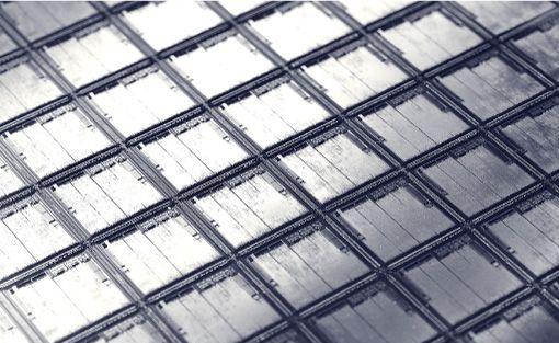
Exaddon technology is compatible with traditional IC and PCB process steps such as photolithography processes, enabling a future of hybrid devices where microscale 3D printing is combined with standard chip processes.
Exaddon's technology can print high-conductivity, microscale structures directly on the traces and contact pads of a microPCB with pinpoint accuracy.
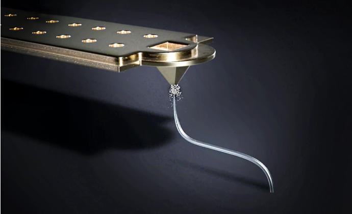
Fine-Pitch Wafer Probing
Access and test pads and bumps at unprecedented pitches using the unique capabilities of 3D microprinting.
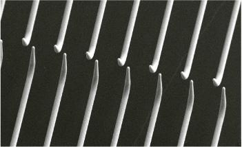
Access <20 µm Pitch
Customizable, template-free printing with great design freedom and array spacing possibilities.
Die Surface Analysis
Dedicated surface mapping functionality for location of 2D/2.5D features ahead of printing.
Exaddon Wafer Probing: Go Beyond Fine Pitch
Overcome the pitch limit facing the semiconductor testing industry and open up new possibilities in chip design and test. The unprecedented capabilities of Exaddon's 3D printing can advance probe testing to new levels by template-free 3D printing directly micro PCBs on substrate carriers.
Discover this industrial application of 3D printing and access <20 µm pitch with 3D microprinted probes.
Discover micro 3D Printed Probes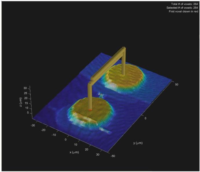
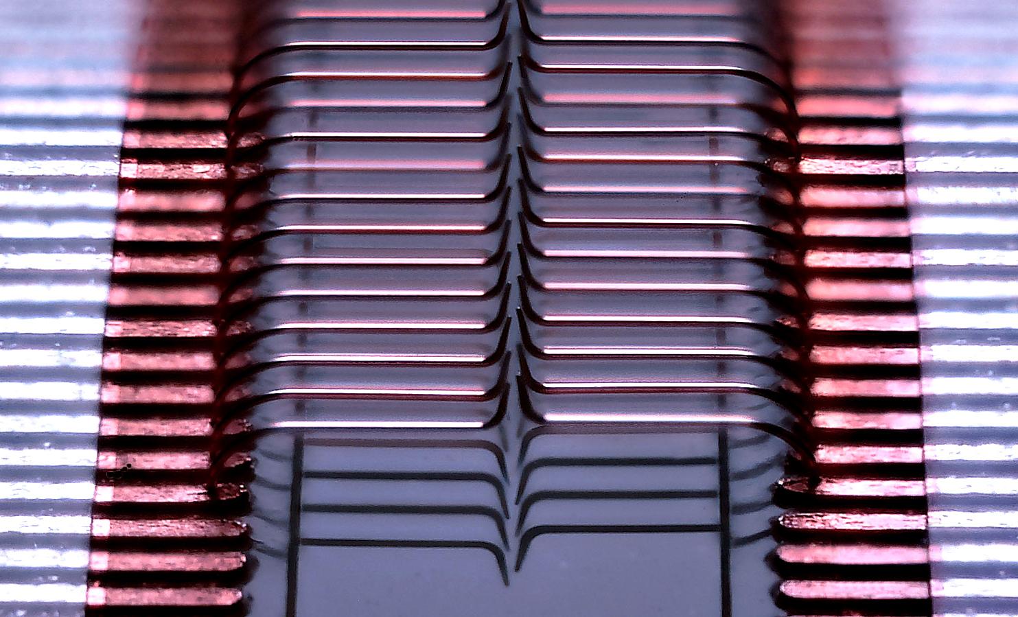
Surface Mapping of 2D / 2.5D Structures
The CERES system allows topographical analysis & surface modification capabilities:
- Location of 2D/2.5D features as little as 200 nm in height
- 3D printing metal microconnectors between contact pads and traces with <1 µm precision
- 3D printing metal 3D microstructures and 2D lines
CERES presents a unique method of modifying surface structures directly on a die, with submicrometer precision.
Explore more microscale 3D printing use cases: Neural Interfaces
Print microscale Neural Needles directly on contact pads.