
The Semiconductor Market is Increasing
In 2022, the global semiconductor market is projected to reach $601.5 billion in annual sales, and the ever-expanding smartphone and 5G/6G markets can be expected to fuel increased demand for the foreseeable future.
Increased smartphone performance is made possible by increased semiconductor device performance, and this has been effected through the continual shrinking of device features without increases in cost or power consumption (per Moore’s law).
Complexity of Semiconductor Fabrication Leads to Defects
Semiconductor fabrication is incredibly complex, and defects are inevitable. Smaller device features mean that the presence of even the tiniest stray particles can cause partial or full gaps in otherwise conductive traces. These gaps, known as “open defects”, would otherwise cause the circuit to short, rendering it useless.

Whether caused by process defects (i.e. parametric yield loss) or particle defects (i.e. catastrophic yield loss), failed dies carry a very large cost to the manufacturers.
Very few viable technologies exist which can repair open defects directly on a die. Commonly, if a die has defects, but still has sufficient functionality for use in less complex applications, it is repurposed.
However, as wafer production is a multilayer process, and die functionality is tested at the end of production, dies which fail to meet yield thresholds will simply be scrapped. This is a hugely costly approach; a company with the capacity to repair open defects and hence increasing the production yield would stand to gain a large financial advantage.
Additive Micromanufacturing: A Prototype Antifuse Solution from Exaddon
During the past three years, Exaddon has conducted extensive R&D into the feasibility of printing antifuses or filling open defects on die surfaces by using its metal additive micromanufacturing (µAM ) technology.
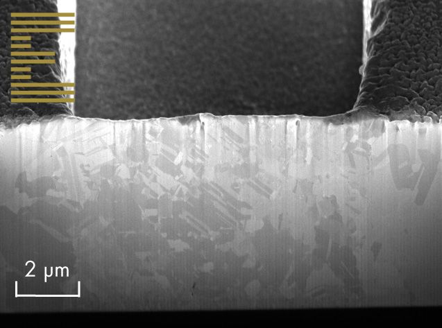
This involves 3D printing microscopic “bridges” or antifuses directly in situ on the die surface, connecting each side of the gaps. These bridges are printed in pure copper, with high conductivity and strength properties.
We are targeting gaps at higher levels, i.e., at the package level where chiplets are connected, such as in the Redistribution Layer (RDL) where the features are much larger than transistor level defects.
Furthermore, creating new connections at this higher level could also be used for tuning analog components, such as resistor values, capacitances and inductances, as well as for testing parts of the circuit.
To be clear, transistor level defects occur in a domain of tens of nanometers. As we specialize in microscale (1 - 1000 µm) additive micromanufacturing, this is not our focus.
A Four Step R&D Process:
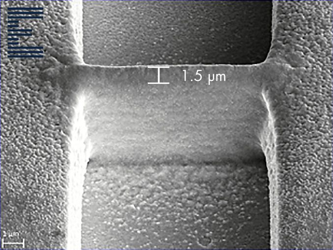
1/ To begin with, the project required Exaddon to design and manufacture a new printing tip to access the trenches, in order that the printed metal contacts each side without voids.
Exaddon’s standard print probe, called an Iontip, has an aperture of only 300 nm, but this was too large, and the tip geometry too oblique to access the sheer sides of the trenches. As such, a new patented Iontip was successfully developed.
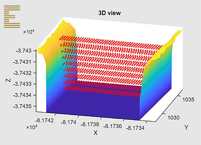
2/ Secondly, the team had to develop a mapping workflow for high precision positioning (< 1 μm) of the printing tip over the print surface. This workflow was developed specifically for 2D and 2.5D objects, i.e. for printing bridges on a semiconductor surface.
The full details can be seen in the Surface Mapping whitepaper, but essentially it allows the user to locate and print a structure with < 1 μm accuracy, directly in situ on the print surface.
4/ Finally, the team are currently involved in step four of the project; developing new routing strategies to achieve good filling and flatness for larger junctions; i.e. bridges with a width in the range of 3-5 μm.
Currently (April 2022), the technology is a functional prototype; trenches of 4 µm or more can be filled with 1-2 μm wide bridges. Whether used for antifuses, packaging, die repair, circuit manufacture, open defect repair, or other applications, there is great scope for further development, and we are very keen to discuss next steps with motivated industrial partners.
Want to discuss this topic further? Get in touch with us via the form below.
Semiconductor Surface Defect Repair with Microscale Metal Additive Manufacturing