
Microscale AM Landscape Overview 2023
Additive Manufacturing as a Subsector
Most industry overviews in the additive manufacturing (AM) media tend to focus on AM companies able to print large objects at large scale.
Popularity defines coverage, and as the majority of AM providers are looking to solve the perennial issues in regular manufacturing workflows and supply chains (such as reducing costs, easing logistical bottlenecks, and expediting prototyping processes), this does make some sense.
This interest is of course reciprocated by conventional manufacturing firms, who are looking to AM with big hopes and expectations of reduced production times and costs.
In 2018, the global manufacturing industry accounted for 16% of the global economy (HP/Kearney), and thus for any AM company looking to this arena, there are obvious target markets, challenges to be addressed, and promising financial returns. The majority of these firms are producing macroscale objects.
Micro- and nanoscale AM has thus far been considered an early stage technology, appropriate for fundamental research, or for solving complex challenges in microelectronics, aerospace, and medicine. For the companies forging new paths in these areas, the playing field is not so obvious, and the media attention not so forthcoming.
Exaddon and its Technology Competitors
Exaddon operates at the microscale, printing complex objects out of pure metal at room temperature. With extensive use cases and collaborations in both research and industrial applications, we have built up an excellent understanding of how a novel technology such as additive micromanufacturing (µAM) can be utilized.
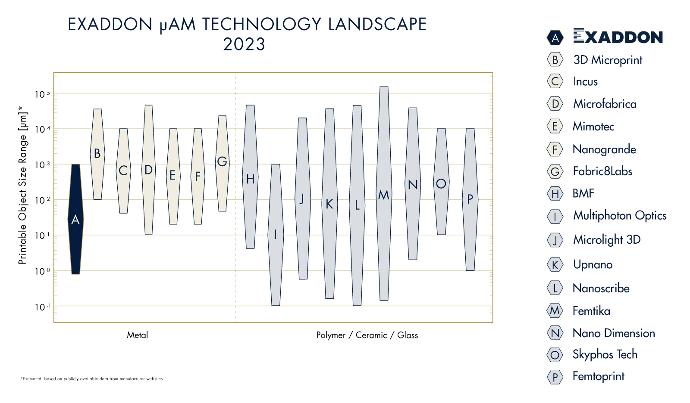
At every object size, whether macro-, meso-, micro-, or nano-, AM can be divided into three main material choices: metal, polymers, and glass/ceramics. Of these, metals and polymers predominate, and each in turn can be subdivided yet further into specific material formulations and print processes.
The applications within high-frequency technology, semiconductors, MEMS, sensors, and connectors are vast, and given the early stage nature of the µAM industry, the scope of potential applications is still very much expanding. For the most part, these fields require the printing of metal parts, often copper (due to its high coulombic efficiency).
Exaddon µAM Landscape
Exaddon occupies a unique position in the µAM space, and this means we can offer unique advantages to those using our technology. There is a complex interplay between the variables involved; print material, object size, and end use case all influence each other. This is discussed below.
Printable Object Size and Print Material
The limits of printable object size differ depending on choice of material. Early stereolithography printers have long been able to produce larger structures, but through the cumulative effect of layer-by-layer photochemical curing of resins into polymers. However, newer polymer 3D printers, such as those using 2-photon polymerisation (2PP), are able to predefine object volume and produce objects with 100 nm resolution, through the use of two tightly confined lasers with a tiny focal volume. Through adaptation of the laser spot size, the voxel size can be changed, enabling mesoscale objects to also be printed.
In terms of 3D printing metal, our matrix shows that aside from Exaddon, companies tend to be limited to the mesoscale. Whilst two providers are able to reach ~500 µm, Exaddon alone has technology capable of producing complex metal objects at sub-micrometer sizes. The implications for this are profound, particularly for the microelectronics industry.
Technology Use Cases
The application of each of these approaches of course starts with the print material used. Medical scientists requiring titanium microparts are not interested in companies which print polymer objects, regardless of their resolution or complexity. Similarly, microelectronics companies requiring copper interconnects are not excited by microscale AM of rhodium or palladium.
Exaddon’s electrodeposition process realizes the lower size limit of 3D printing of metals; to go smaller would be to enter 2D printing. As such, we are in the special position of being able to offer a unique technology with unique application.
The image below demonstrates the scale of our printing tip technology
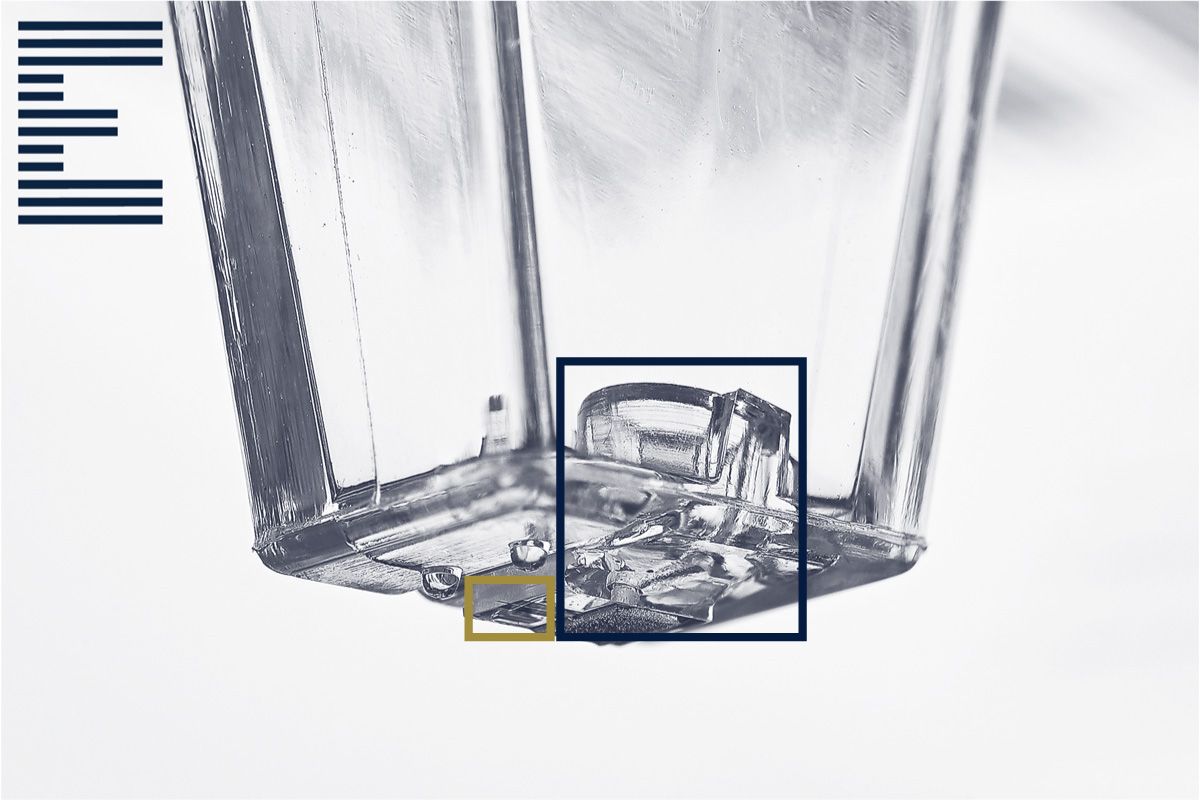
The reservoir contains just 1 µl of 'ink', which is pushed through to the actual printing tip and onto the print substrate via an applied pressure which can be changed dynamically while printing. This 'ink' (as we refer to it) is ionic metal, which is then reduced to solid metal atoms during the print process. Learn more about our printing process here.
Of course, 1 µl is 1'000'000'000 µm3, which means that depending on the chosen object(s) to be printed, one reservoir of ink can be used to print many objects. The almost infinitesimally tiny printing tip, in essence a hollow AFM cantilever, has an aperture of just 300 nm in diameter, out of which ionic metal (typically copper) is deposited electrochemically.
It is through this technology, and the years of testing and refinement behind it, which enables Exaddon to occupy a unique position within the µAM space. Accordingly, we offer a unique solution to a range of use cases, which necessarily cannot be matched elsewhere.
Reach out to us and learn more
Discuss your industrial applications or fundamental research challenges
Additive Manufacturing at the Microscale